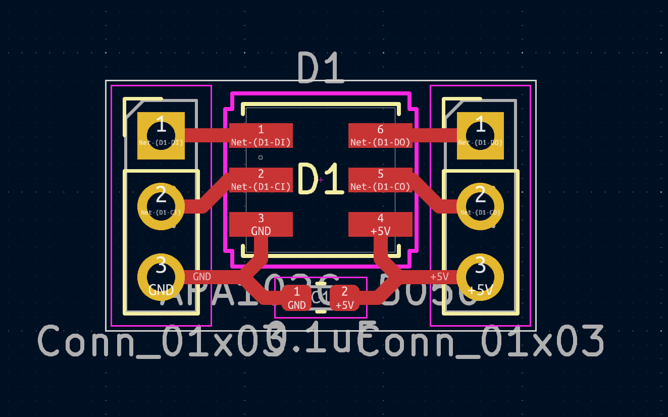
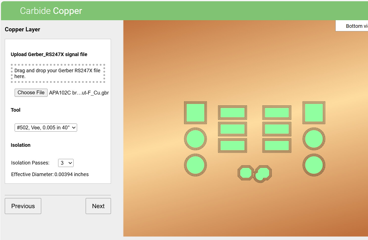
So, I’ve designed a quick breakout board for a 6 pin SMD LED specifically for the APA102C LED. When I import the Gerber files for the Front Side Copper, it loads the pads, but then seems to get the traces confused and loads no traces, but places a blob in the wrong place.
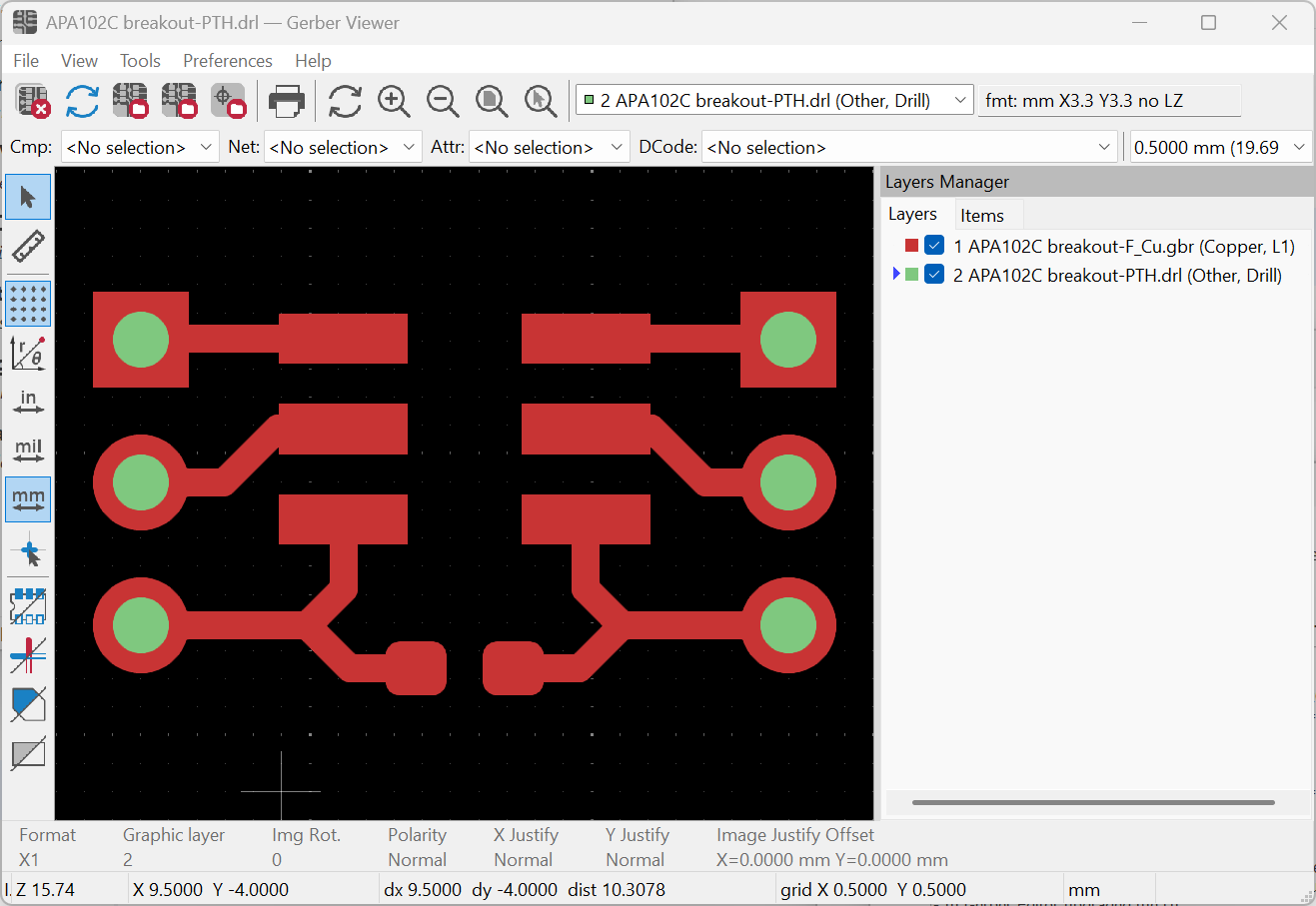
Checking the gerber files in a viewer appear to be correct. Checking the gerber files in Flatcam also seem to be correct.
APA102C breakout_KiCadproject.zip (13.6 KB)
APA102C breakout-F_Cu.zip (1.2 KB)
I’ve had success with Carbide Copper with KiCad 7.0 on a similar board, and this same project upgraded in KiCad 8.0 still works. But any new KiCAD 8.0 project always seems to have issues bringing the traces into Carbide Copper. I’ve tried various options while generating the Gerber files, but haven’t been able to get KiCad 8.0 to generate a file that Carbide Copper loads properly.
I know I can use Flatcam to do this, but for small single sided boards I figured Carbide Copper could be a quicker tool.