Using Eagle 9.6.2 Standard and Carbide Motion Build 536.
I’m have no problems saving the CAM data for the bottom copper, but the drill file is another matter. The default drill file of course does not include drill holes, only mount holes. I modified the CAM output to use the “PCB stack” which correctly included all of the drill holes - per the preview, however when running this file in Carbide Motion the spindle never turns on.
Someone mentioned Carbide CAM output, but I do not see any such settings in Eagle.
Hoping to get this sorted so that I won’t have to ruin another perfectly milled PCB. What is everyone else using? I also exported the holes as DXF, imported into Carbide Create, flipped the image and exported the gcode file. This almost worked but for some reason the holes were off by about 1.5 mm.
What’s the output type? I’ve been using Eagle for maybe 25 years now and have no problems like that. However I’m sending files out for fabrication. Gerber 274-x for the layers and Excellon for the drill file. One thing that has happened over the years is sometimes the CAM files use one resolution for the Gerber (say 3.4) and another for the drills (2.3) which when you preview the files in things like GerbTool cause the drill file to be represented miniscule.
If you are using Gerber files and Excellon files get a previewer and check the files.
I’ve only used Eagle for about five years and have sent out one design for fabrication, but in this case I am attempting to generate a one-off circuit board, which I will do as a hobbyist most of the time.
I attempted to use the ULP pcb g-code plugin for Eagle, but that made matters worse. Four gcode styles are available. Three were not compatible and one was simply a reversed coordinate system.
So, without a compatible Carbide style for the plugin I reverted back to the standard CAM Output processing. Now the spindle is not even turning on for the copper traces.
Here are the top portions of two files. The first from Eagle, and the second from Copper. Notice that the Copper output does not have any spindle control, however at the end of the file it does send M05 to stop. The Fault codes surely mean something but I’m not familiar enough with these tools to know where things might have gone wrong.
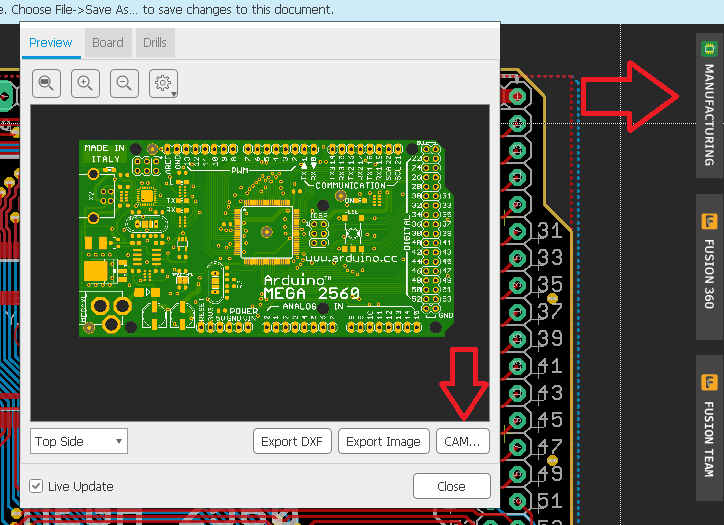
Don’t use the ULP. Likely it has a bug. Use the “Manufacturing” tab on the far right. If this tab is turned off, it can be found under the File menu as the CAM processor. The manufacturing tab is nice however because it can give a quick pre-view of the board.
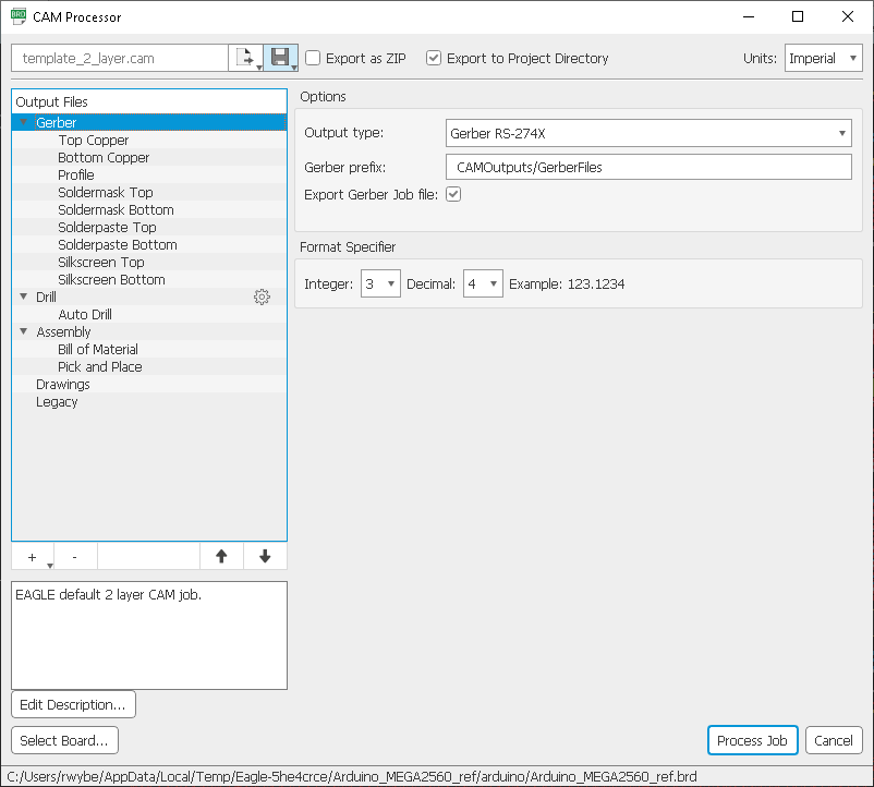
The default 2 and 4 layer CAM files work reasonably well but you may need to change the units from Metric to Imperial.
It should produce the necessary gerber files and NC drill file. A sample of the NC drill file should look like this:
M48
;GenerationSoftware,Autodesk,EAGLE,9.6.2*%
;CreationDate,2021-04-19T04:00:21Z*%
FMAT,2
ICI,OFF
INCH,TZ,000.0000
T7C0.0160
T6C0.0240
T5C0.0374
T4C0.0400
T3C0.0866
T2C0.1260
T1C0.1300
%
G90
M72
T1
X4600Y3270
X2240Y3270
X3420Y1300
T2
X38000Y1000
X6000Y20000
X35500Y20000
X5500Y1000
X26000Y14000
X26000Y3000
T3
X1500Y17362
X1500Y12638
T4
Thanks for that. Changing both the Gerber and Drill setups to imperial seems to have made a difference, but there is still no spindle control. I cannot fathom why, as it worked in the past. Inserting:
M03 S10000
after each tool change will have to do for now.
I also realized that the Eagle CAM Output has been integrated into Fusion 360 in the “Electronics” design. There is some real possibility there, as it is already referencing Carbide Gerbl. If I can get the toolpath operations set up we might have something. I’ll let you know how that works out.
I don’t access Eagle from the Fusion 360 side. I run it stand alone and only export to Fusion as needed.
More features seem available this way. Further, doing it this way avoids the cloud storage issues. Since some of our work has express restrictions on cloud storage for reasons of controlling the IP. And finally, been using Eagle since the 90’s, way before Autodesk bought them. Like some of the upgrades but so used to the goofy Cadsoft designed interface I don’t even notice it until I try to explain how to do something!
I should also add that I’m not cutting circuit boards with my Shapeoko. I have an older LPKF ProtoMat for that. That software takes in the gerber and NCD files and generates the necessary gcode to run the machine. Their software manages the feeds and speeds.
Even at nearly 30 years old, it is still doing a stellar job on two sided boards. Only use it in “emergencies” when we need to test something next day or make up a “bugger board” to make fixing a production mistake easier.
It turned out well with a few hand fixes to the nc files. I’ll follow up sometime in the future if there’s anything to report, especially in regards to Fusion 360.
FYI, a trick for removing large areas of copper is not to do it with your mill. Instead put a large flat tip in your soldering iron. Heat up a corner of copper you want to remove and pick at it with an Xacto blade. The heat will soften the adhesive on the foil and voila, it peels right off. Usually faster than voiding lare areas with a mill.
Generally when I’m milling boards on my Protomat using their post processor for Gerber files, the result is such that I don’t remove large un-routed areas of copper. Instead traces have paths created around them to isolate them from the foil. Unless there is a good design reason to void the copper, I simply don’t. Or as mentioned above, I’ll use the heat and peel method. Small islands of copper, like 1mm^2 and smaller I do allow the mill to remove simply because they can come loose and you probably don’t need the headache of a small bit of copper flopping around on your circuit.
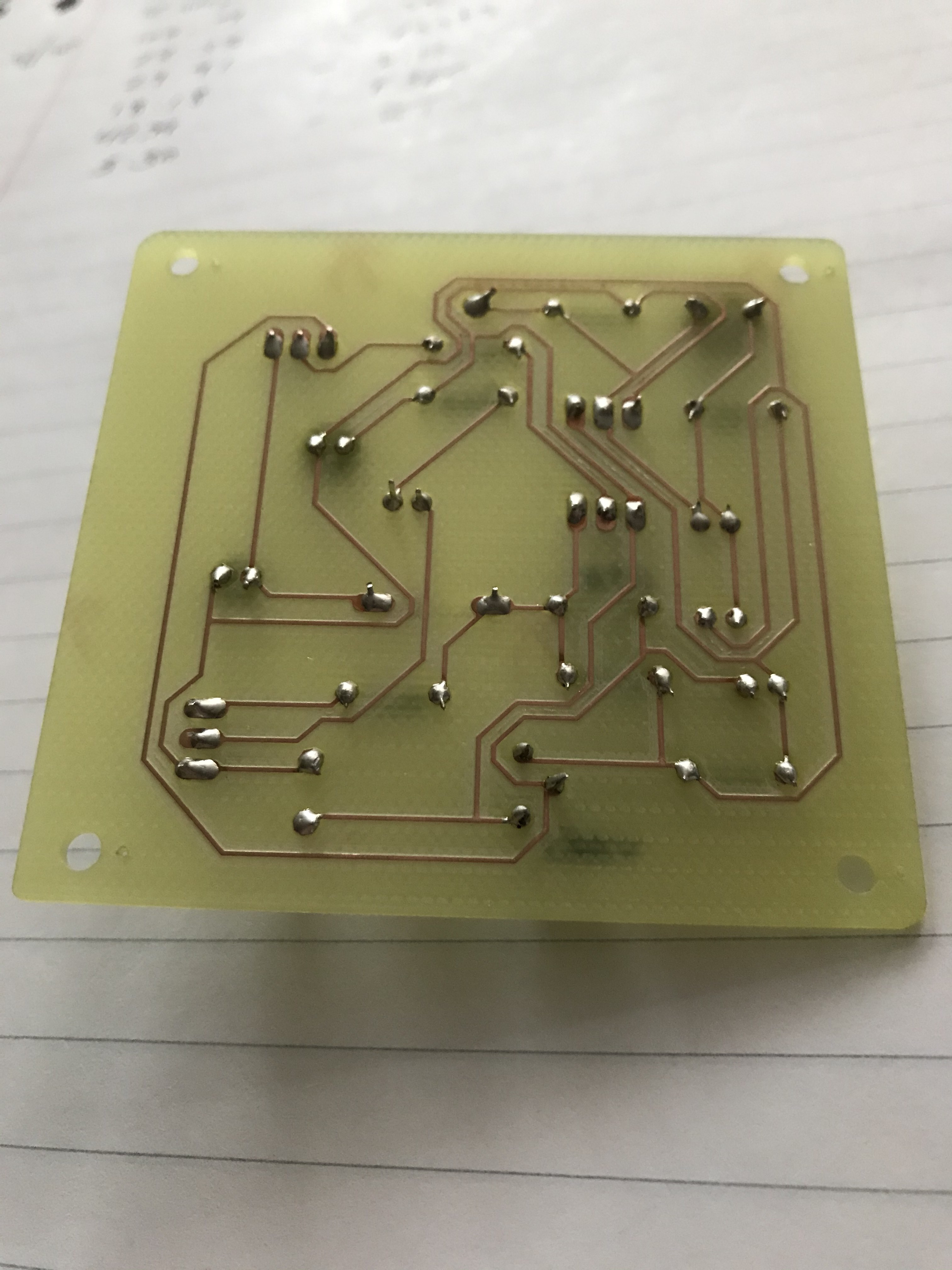
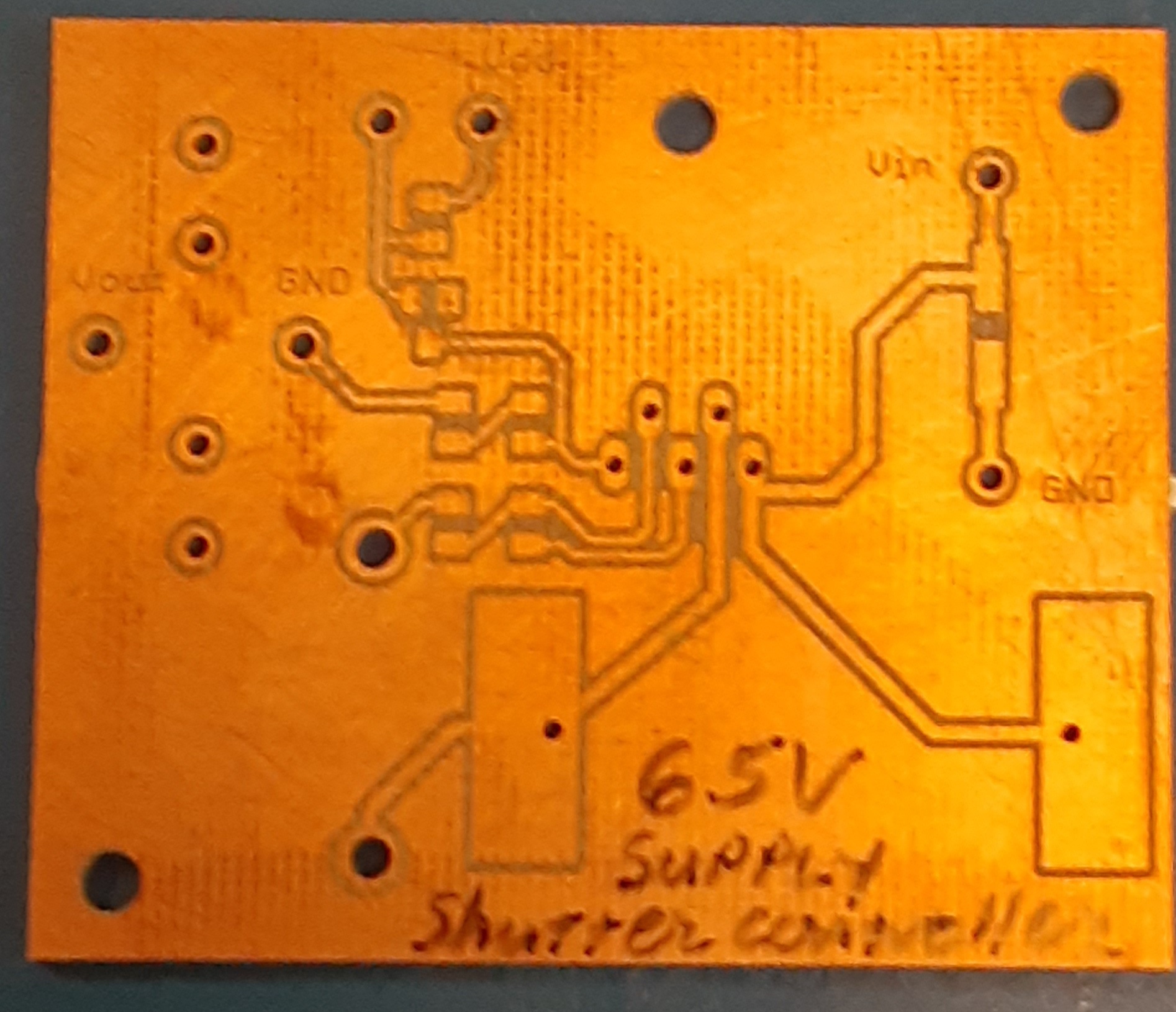
Here’s a quick and crummy cell phone snap of a spare board I made. It was for a 65V switching power supply we were developing for an inductive load (solenoid controlling a large shutter). I think this board has been kicking around the lab for about 10 years so developed quite a patina. But you can see how I just milled enough material to isolate pads and traces.
Also, this is a two sided board, the bottom side being a ground plane and a few traces. So some of the holes are vias that connect to the back side. Since I don’t have the gear to plate the holes I just insert a fine wire and solder top and bottom.
Based on the size of this board, the number & different sizes of drills, it was probably about 20-30 minutes to fabricate. I probably panelized two or more of them when it was done just to have a couple spares to experiment on.
I just found the bug I was looking for. I fell into the habit of saving the Copper outputs as separate files - and which have no spindle control. Same CAM inputs were processed by Copper and saved as a single nc file - that one contains spindle control.