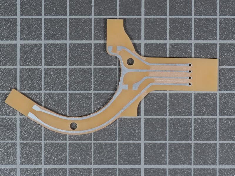
While most of the discussion of PCB production seems to be around the Nomad, the HDM will do a nice job. I have done a number of circuit boards using Carbide Copper. But Carbide Copper does not handle curved traces well. I thought it might be interesting to post the results of using Carbide Create Pro to create this circuit board used in a proof-of-principal instrument I am building. It is not as beautiful as a fab house board, but it only took a couple of hours on the HDM (45 min of which was cutting time) and the board was available for testing. The fab house would have taken a week, had a minimum quantity and added a special routing charge for the odd shape. The grid in the photo is 1cm.
The board was laid out in SolidWorks, exported as a DXF drawing and then cleaned up and converted to SVG in Inkscape. The board was cut using REST programming with successive 1/8, 1/16 and 502 vee bits. The "scrubbed area is the 502 cuts. There is some necking that I could probably eliminate by running a calibration test for the effective diameter of the 502. The path calculation in CC Pro is different than Carbide Copper. I prefer the latter for traces. It would nice to incorporate some of the Carbide Cu logic into Carbide Create, but I suspect there are enough differences to make it not worth the effort.