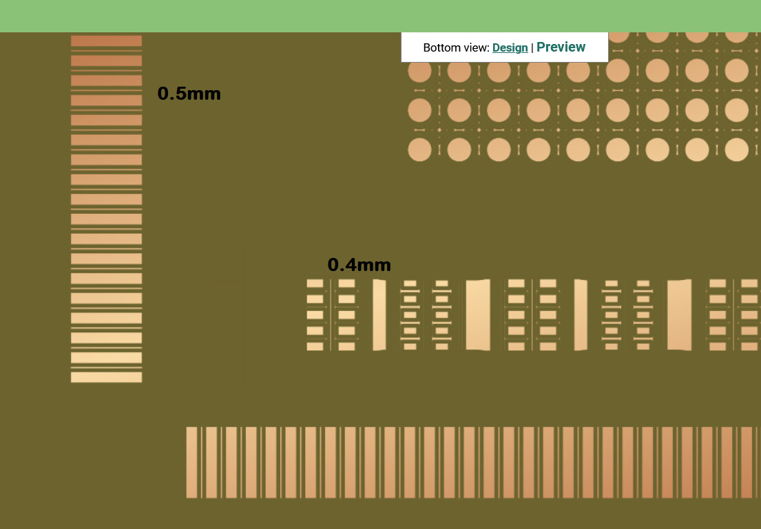
I’m trying to evaluate whether my original Nomad is capable of cutting pad traces for an 0.4mm pitch connector before I go much further. Anyone know of any sample files I could download to test? Seems like the #502 Vee has an effective diameter down to 0.1mm but wanted to see for myself.
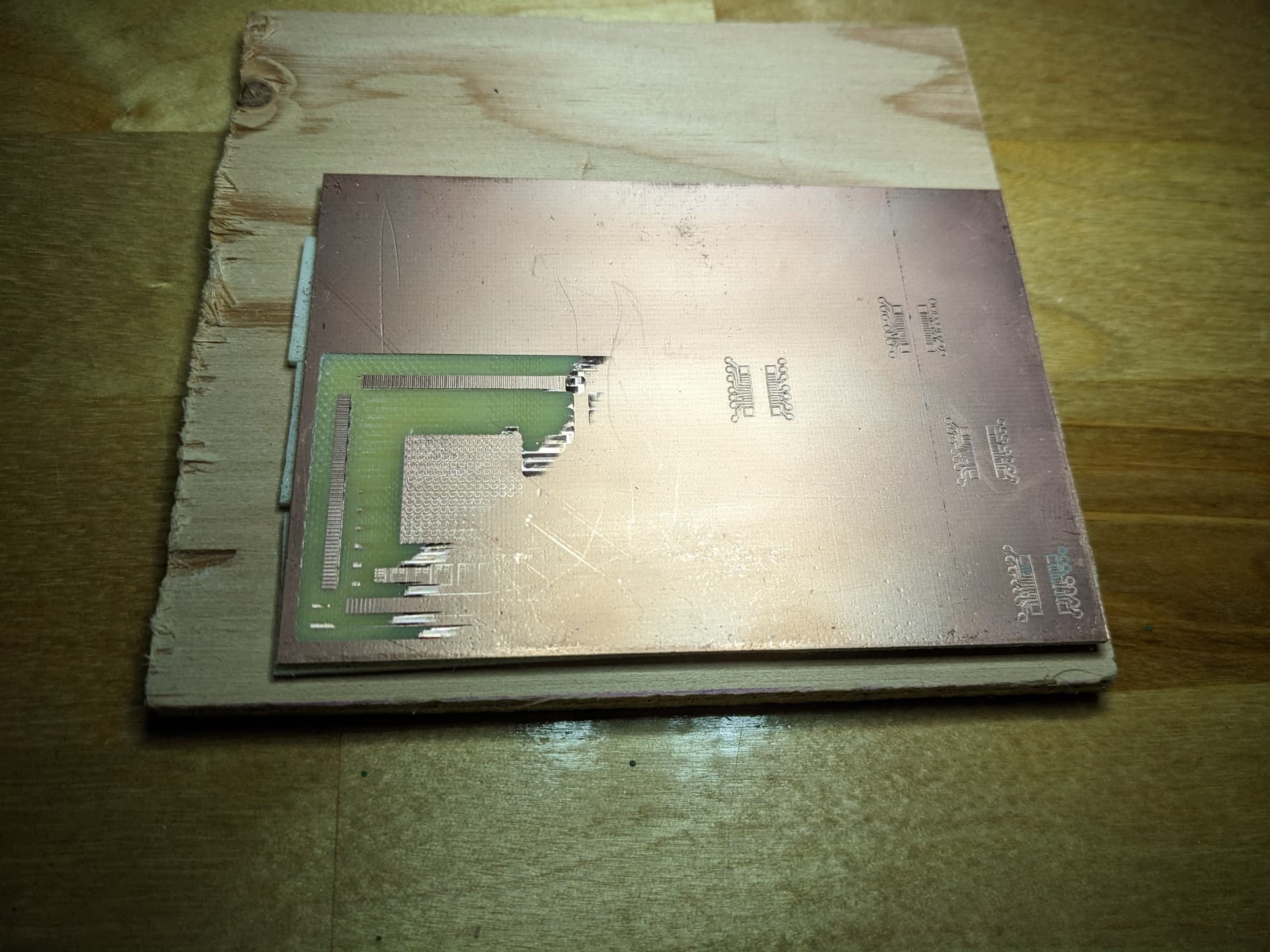
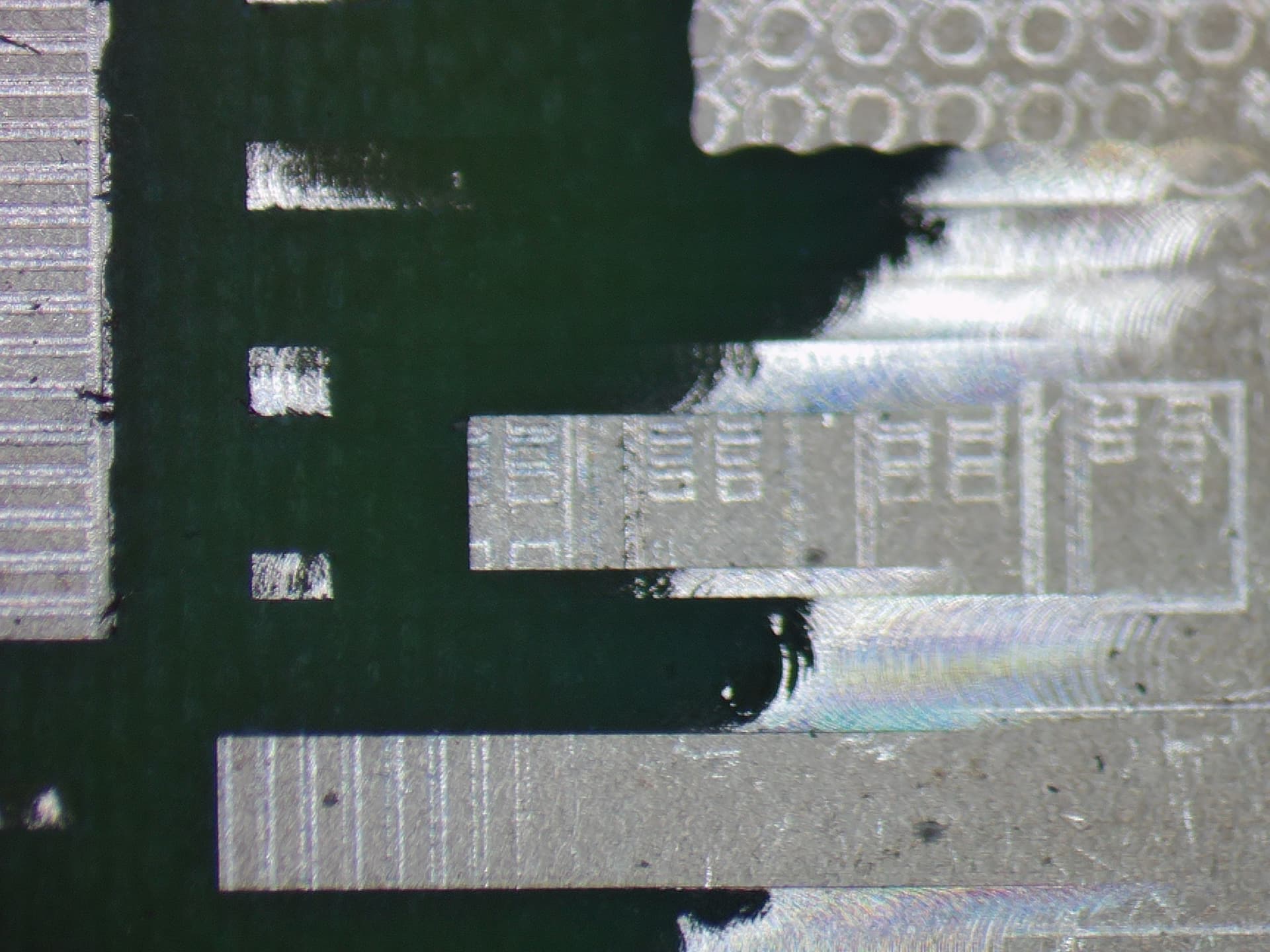
Unfortunately I wasn’t able to get even close to the model result above. I set the 502 bit right onto the copper, verified with a continuity probe, and it still doesn’t look like it cut deep enough. Without a perfect fixturing system or a depth contour map of the surface I’m not sure how to ensure that all regions of the board get cut properly.
What tips/tricks are you guys using to get effective results?
PCB milling is typically quite challenging because any minute variation in depth/evenness will result in engraving too deep or not enough, as you experienced.
The killer solution for this is to use software that has surface mapping capability, I know of bCNC that has this feature (“autoleveling”) but have never used it myself.
If you cannot do that, the next best thing would be to mount your PCB on a jig/support that is adjustable in height at each corner, and manually tune it (maybe using shims under the corners) and checking by touching off the surface with the engraver itself in multiple places (i.e. paper method of zeroing) until it touches the surface in all places at the same Z value. Tedious, but doable.
If you cannot do that either, the least you MUST do is surfacing the support where you will install your PCB, to have a reference plane that is known to be parallel to the machine axes. This scrap of wood you installed the PCB on is probably not evenly flat. Surfacing the wasteboard/support goes a long way. But then of course it becomes a matter of whether your PCB blank itself is flat enough. Don’t use thick double-sided tape either. You can probably lay the PCB flat on the surfaced wasteboard, and use tape to hold it in place. The milling effort is very minimal, the pcb won’t move and the tape won’t get in the way if you put it on the sides.
I realized that my bed wasn’t level at the least so my plywood/foam mounting wasn’t appropriate in the least but I was hoping that it might carve something representative near the starting point I measured zero at.
I’ve installed bCNC and have it ready to go, just need someone at C3D to list how I can tweak my original 883 to add the wire clip probe, email is their tech support mailbox