Testing out Carbide Copper

I finally got around to running a test cut using Carbide Copper on my Shapeoko 3 today, and I thought I’d post some pictures and a few notes.

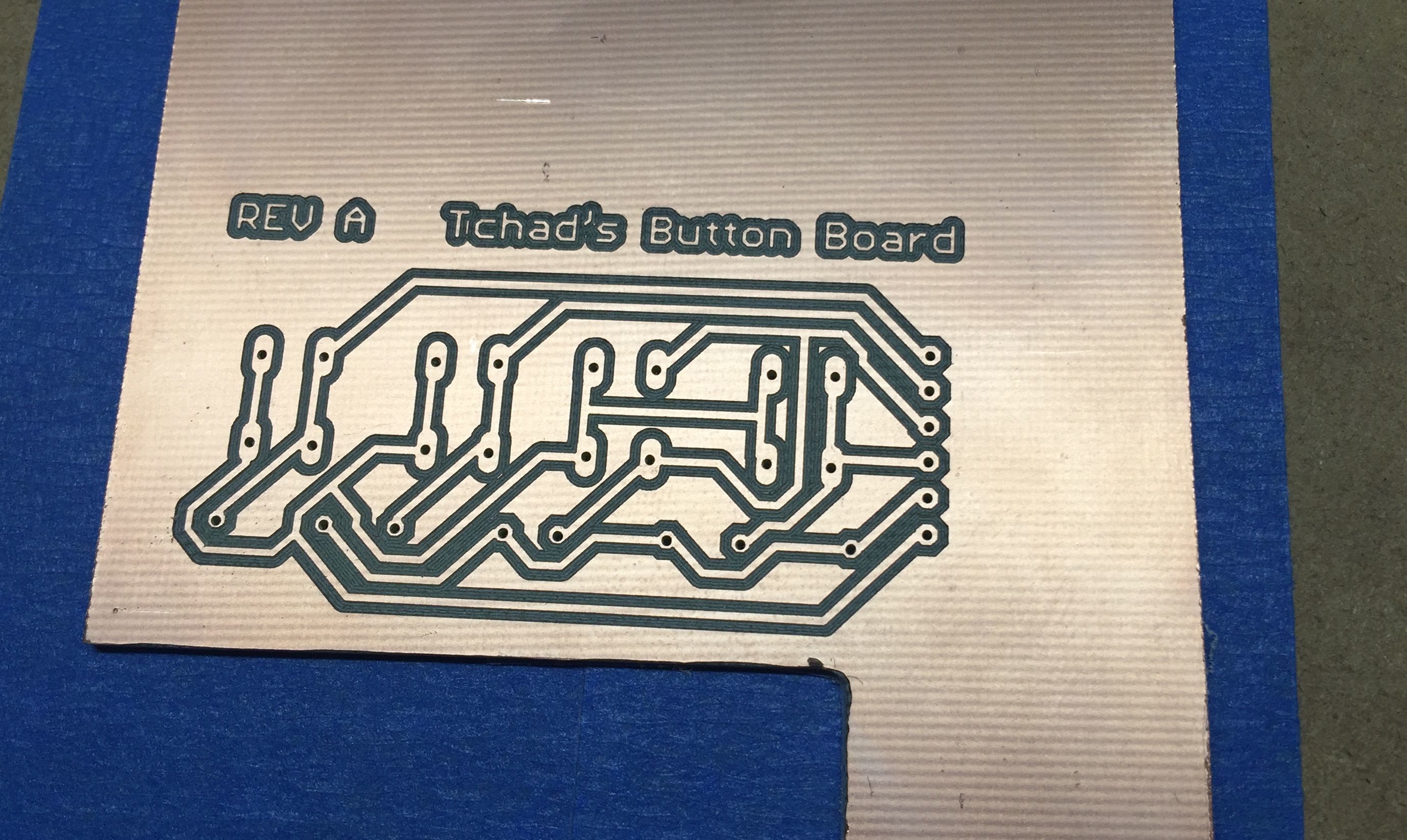
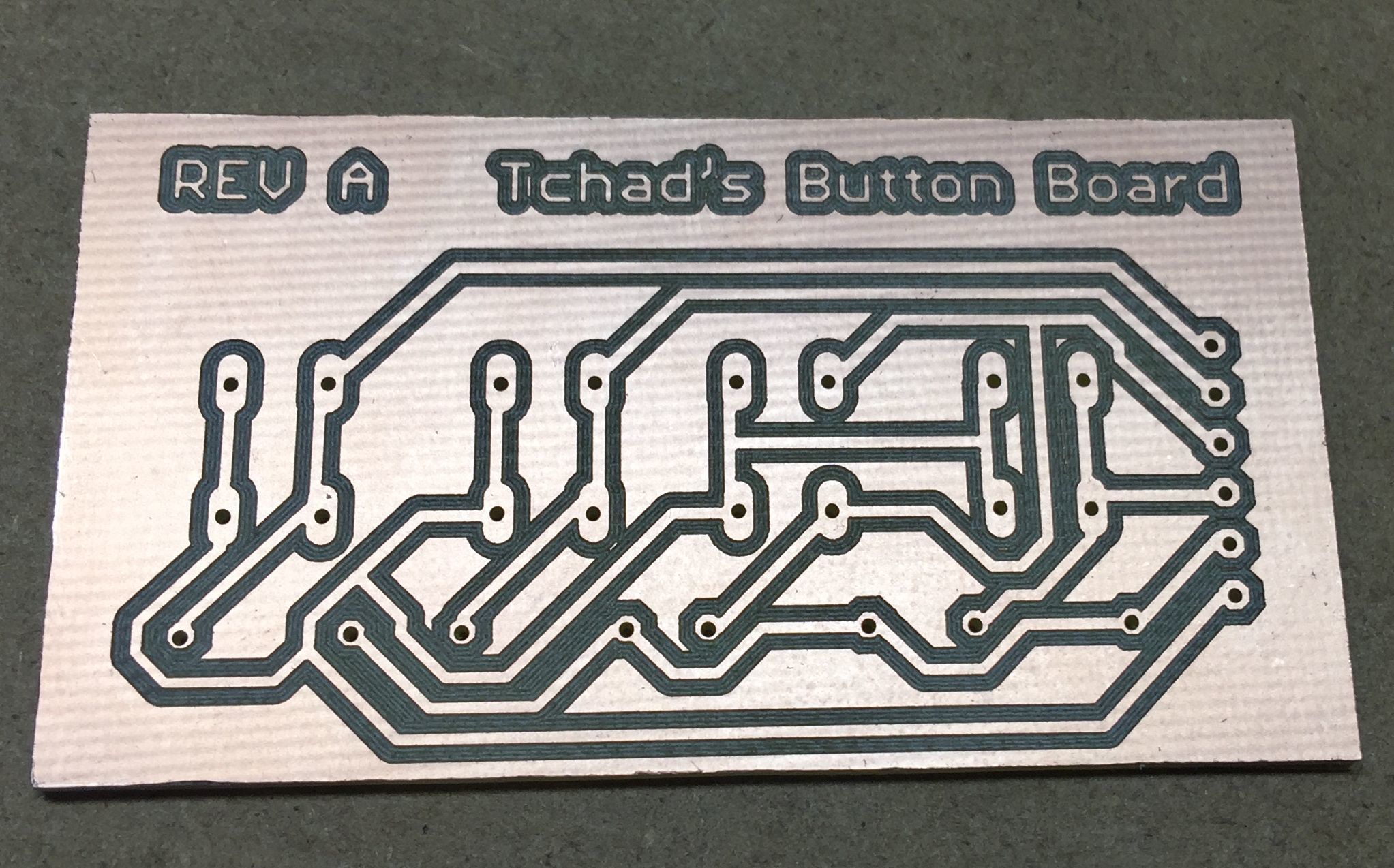
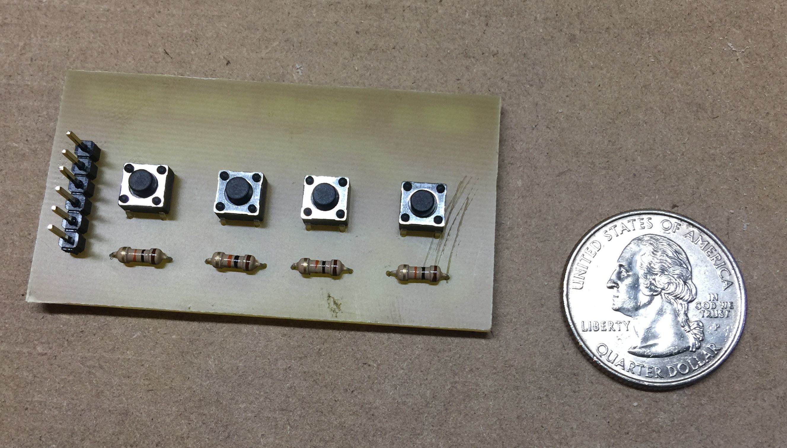
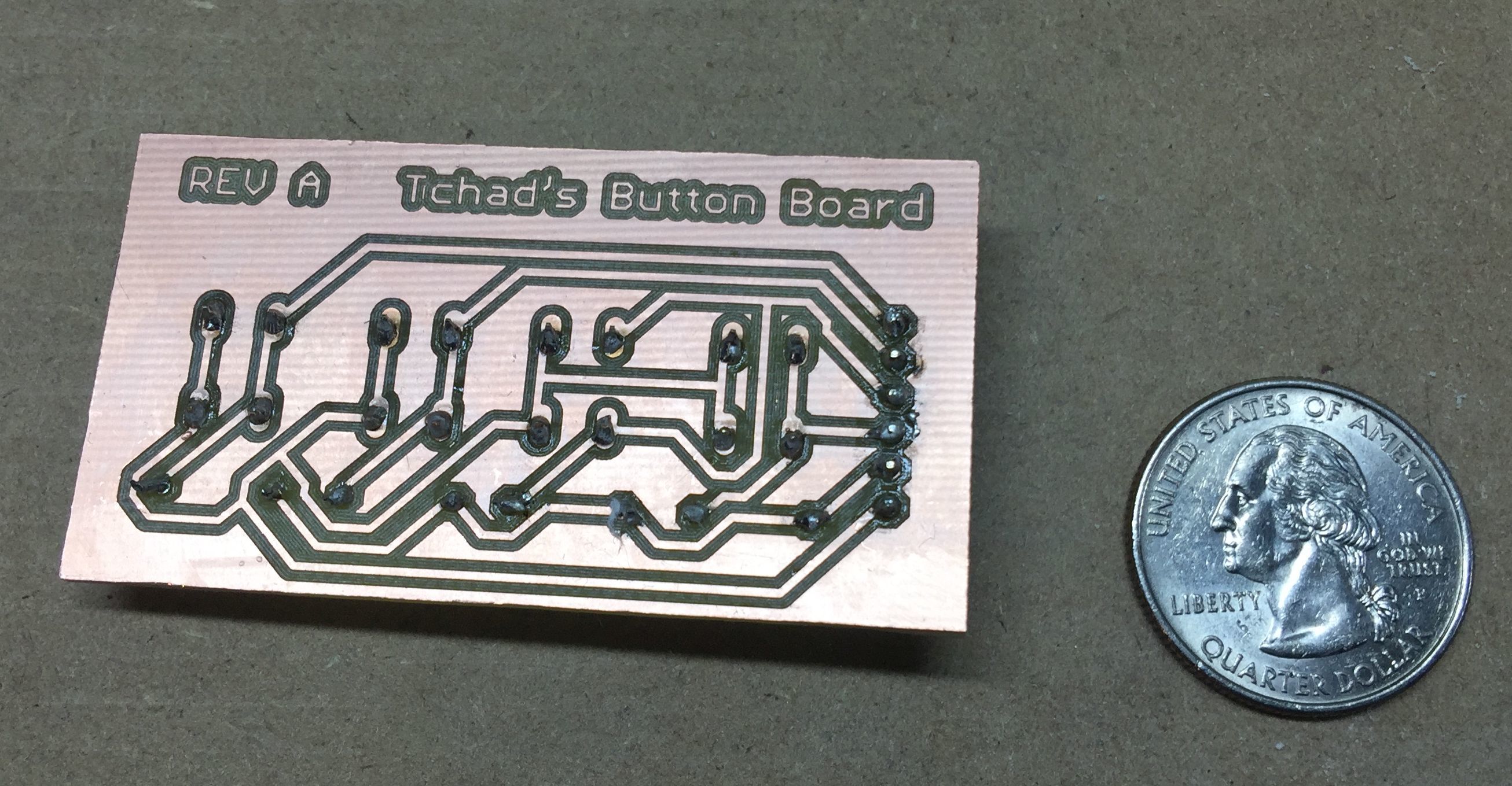
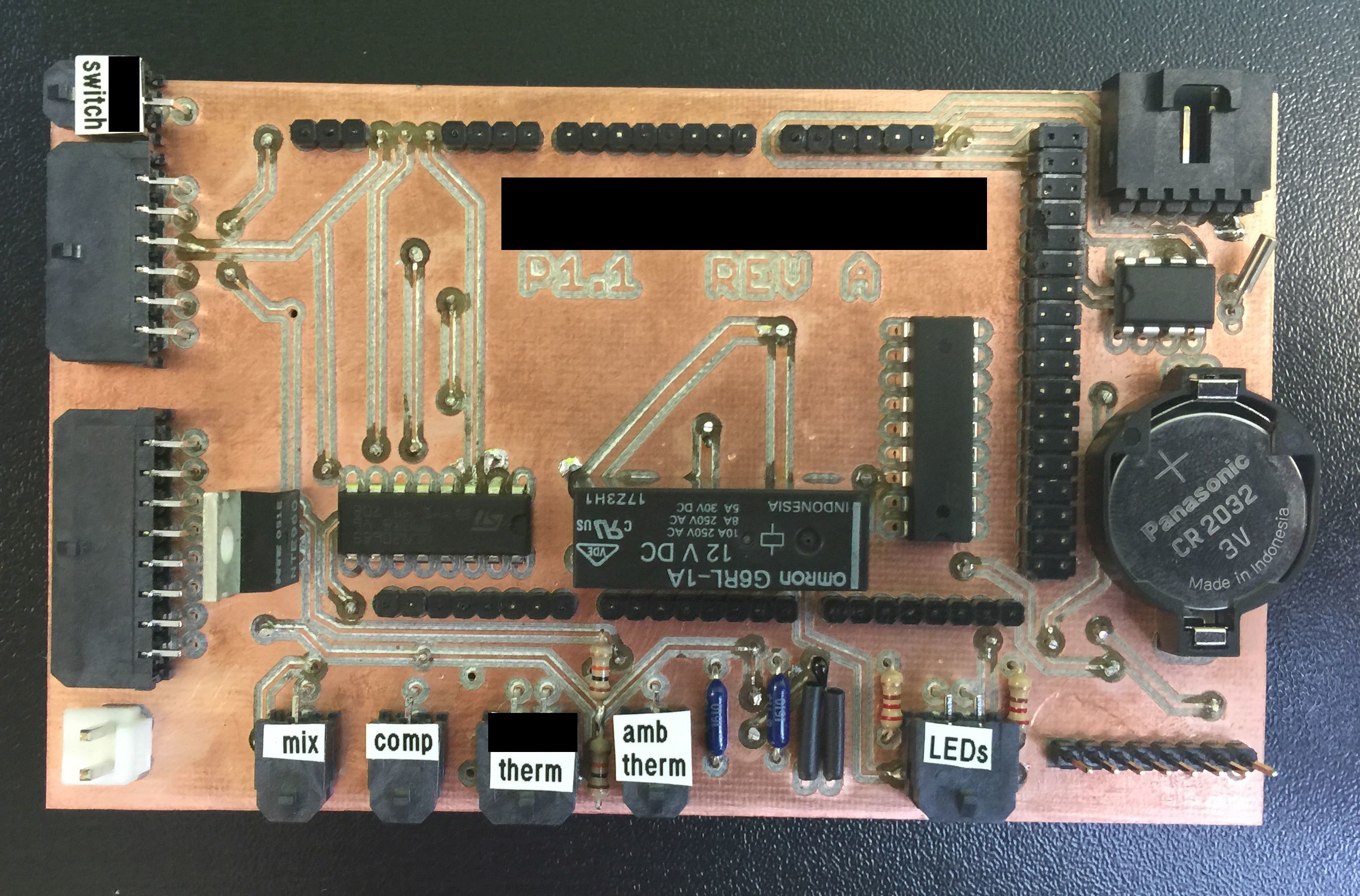
This simple button board was designed in Eagle 8.2.2. I plan to use it when tinkering around with an Arduino, so the 10k resistors are pull-down resistors to keep logical low consistent.

I missed the initial sale of FR1 copper clad, so the board I used is FR4 from Mouser.

I cut it on my Shapeoko 3 with the DeWalt 611 set to 3.5 (~21,000 RPM) (not because I know what I’m doing, just because that’s what I set it to… and it worked fine.)

I used Carbide Motion to run the job, and I manually split the gcode file into three files, for the etching, drilling, and cut out, so that I could re-zero the Z axis during tool changes.

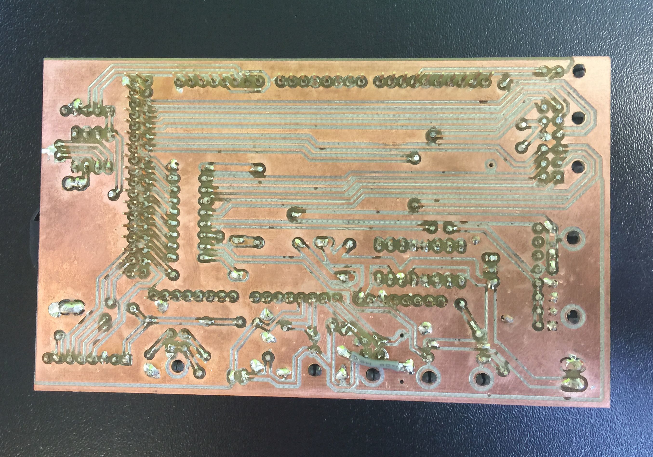
As @jimmo mentioned in another thread already, having a super flat waste board is crucial, and variations in the thickness of the PCB can cause some trouble. I resurfaced my waste board, then attached the PCB, and still found .002 variation. I increased the size of the traces and clearances slightly [1] and then deliberately zeroed my machine about .002 too deep. This will probably affect the life of the cutter (doubly so because I’m using FR4), but for a nice clean PCB it’s worth it.

[1] The board in the picture is cut with traces set to 25mil and clearances set to 30mil (in reality, the traces are probably a little narrower, and the clearances a little wider, because I’m deliberately cutting a little deeper). In retrospect, these are too conservative. I’ll probably go back down to ~20mil for each. I’ll also probably increase the size of the pads next time, my soldering skills aren’t good enough for those tiny pads!

The Carbide 3D bits, specifically the drill bits, are the cat’s meow. Watching it drill those tiny holes so quickly and easily was impressive.

So based on my initial run… I’m impressed, and I’m glad that I dropped a little money to buy the drill bits and PCB engraving bits.

I have a much more complex PCB project coming up. I’ll post pictures of that in a few weeks.

9 Likes

I also break up the process so I can reset the Z zero. The program does not allow enough processes (just two, rough and finish) for me to make my dies properly.

I have a rough pass, a second rough pass, a finish pass, a canned hole drilling cycle, and a etching pass. All separate programs. It just makes it all easier to do it that way.

I love your button board. Excellent work!
one thing I wish carbide3d would do is make a spindle that goes beyond 10k rpm. those tiny tools need 15 to 20k rpm to function properly.

1 Like

I have some questions to ask from the bowels of ignorance. Why does the depth of cut matter? I can understand if you’re using a vee bit because deeper means wider, but if you used a very small straight bit, it wouldn’t matter, would it? Don’t you just want to cut through the copper layer? My second question is more involved and probably beyond the scope of CNC. I have a button box design for my Logitech G27 steering wheel. I built the thing from plastic and made “traces” using copper foil (what some people describe as trailer park electronics design). The point is that the location of the buttons is critical. For no reason whatsoever, I expected that in a program like Eagle I could import a background image/template of the button layout and then build the circuit around that, but it doesn’t seem like it works that say. Anyway, in the end, it looked like the learning curve to do one PCB wasn’t going to be worth the effort. I guess, in a nutshell and as simply as possible, how does one design a PCB layout where the location of the parts is critical? For illustration, here’s the button board for my wheel. http://imgur.com/M543VoL and http://imgur.com/VKWnL3O

1 Like

Interesting! I’ll try faster next time. Since I’m using a Shapeoko, the spindle does go faster… I’ll try it and let you know how it goes.

It’s all about chip clearance and heat removal. That’s why I use a jet of air on the tool… it clears the chips (death for a tool) and keeps the heat down. I never run any of my tools at less than 10k rpm, unless I’m running plastic or something. That’s the time for lower RPMs, and heat removal is critical (plastic products melt).

1 Like

You’re right - with a very small straight bit, it wouldn’t matter. I’m using the #501 PCB Engraver, which is a 60 degree V with a .005 tip, so deeper implies wider as well. As far as I know, there isn’t such a thing as a straight bit that is small enough for PCB work, but I’m also very noob at this and don’t have a full understanding of what is out there.

Wow, your “trailer park electronics design” steering wheel is impressive! I can imagine the effort it takes to put down the traces straight and clean. It’s also way nicer looking than running wires!

You may be right for your purpose (your foil traces looks great, I’m not convinced that a cut PCB is actually an improvement over what you already have) I will say that the learning curve for Eagle isn’t too bad. If you know how to use Photoshop or Gimp (layers), and know basic electronics design, then you’re more than 1/2 way to being able to use Eagle. I followed Jeremy Blum’s Eagle tutorials on YouTube (the first one is here.) They are for a previous version of Eagle (before AutoDesk owned it) so all of the icons are different, but how everything works, so far, is exactly the same. I spent one long day going from zero to finished circuit. I watched about 1 hour of tutorial videos through twice, first videos 1 and 2 from start to end, then again bouncing back and forth between the video and my Eagle design to try it out. I’m definitely not proficient at it yet, but I can get it done.

This is the first circuit I’ve ever designed in Eagle… I learned it two days ago, so others with more experience may be able to chime in here. I’m not aware of a way to import a raster image to use as a template, but Eagle does have a very precise and configurable grid in the board layout view, so theoretically you should be able to import the wheel’s dimensions and work from them. It supports DXF import, so if you could scan a picture of the base into something like AutoDesk Fusion 360 (or any other CAD program that exports DXF), trace it and scale it, then export a DXF, you should be in business. Otherwise, you could manually draw some scaled polygonal outlines of the main board shapes in Eagle to create your own template. Other than that… hopefully someone with more Eagle experience can chime in!

1 Like

Did you manually separate the G-code runs, or does copper now support multi-tool segregation of your G-code?

I manually separated them. I saw somewhere on this forum that that feature is coming, but it’s not there yet.

Here are a couple of images of my more involved project. It’s a 3x5" Arduino shield that breaks out a handful of sensors, LEDs and buttons via Molex connectors.

Unfortunately, I forgot to take a picture while it was in the pristine freshly cut condition, so you have bear witness to my messy soldering. :slight_smile:

The gcode is created with Carbide Copper, but I ended up using bCNC to cut it, both for the auto-level function, and for the optical gcode alignment function (using a USB camera mounted on the spindle) so I could align the second side of the PCB without alignment holes / pins (because I use a vacuum table to cut these, and I don’t want to bore holes in it for alignment pins!)

Interestingly, Copper generates a .1mm deep etching. With the (simulated) perfectly flat surface after running the auto-level probing function in bCNC, .05 mm yielded much better results, so I’ve been zeroing my tool .05 mm above the surface of the board before cutting it.

Now that I have two-sided PBC milling down pretty well, my next project will involve copper plating the through-holes, so I’ll drill first, then plate the holes, and then mill both sides. More to come!

3 Likes

Nice work and great info too… looking forward to your plating efforts.

P.S. your soldering is nice considering it’s bare copper with no masking.

1 Like

You’re making control boards for old machines… The one shown is suspiciously like the board I just replaced in a big mixer… heh heh.

You’re not far off!

After this project, I have more confidence that I probably could make a new control board for an old machine, as long as the communication protocol was documented. Not that it would be easy, reverse engineering proprietary firmware would be an interesting challenge. It would have to be a valuable machine with no other way to replace the board to make the effort worthwhile.

This has been a bigger project than I anticipated. I originally thought it would take a week, it’s been more like a month.

I have completed my through-plated boards now too, so I’ll post more here once I wrap everything up.

1 Like

I wonder when you can attach a soldering iron with solder feeder to the router holder on a Nomad or SO3 so as to CNC-solder components to the PCB? Not like pick and place, but more like "point solder"components to the PCB? I’m not a mechanical engineer, but it seems like the next step for precision prosumer / hobby soldering? BTW, I can solder with some accuracy, but my electronics skills are in their infancy stage.

The biggest problem I find is failure of easily replaced components, and simply broken boards. You could have a nice little side business if people could send you a picture of their old board.

1 Like

It seems like it would be possible, but it would be challenging due the amount of variation in components, angles, amount of time for the solder to liquefy etc.

One potentially easier way to do something like that would be to use all surface mount components, and build a CNC solder-paste applier. You’d still have to manually pick and place the components into the solder paste, and then reflow with a heat gun or oven, but if you had a large number of SMDs, applying the paste in an automated fashion would be pretty cool. Then again, with the low number of boards that I hand solder, I know I would never recoup the time I spent creating the automation tool. It would just be a fun project. :smiley:

I love this stuff… the level of difficulty for building pretty awesome automated tools has come WAY down in the last 10 years.

1 Like

First try with Copper. I used ChiliPeppr for the Auto-Level feature, worked pretty well.

The custom cutter feature is needed, as I had to pick from the Carbide3D cutters, 0.010" 60deg V-bit, but the cutter I used was a 0.006" 60deg V-bit.

You don’t realize how much solder mask helps until you have to solder 0603 resistors and caps without it :slight_smile:

The board works great, it is a PIC with ICD header to drive WS2812 LEDs for an Acrylic sign.

3 Likes

Nice work!

Were all of your components SMD? I very much agree about soldermask, but through-hole (on my design) was probably a bit easier to solder, if just because the pads are physically larger, and the components are held in place while you’re soldering.

I tried solder paste with a heat gun also, it works fairly well, but getting the temp, time, and fan setting right takes some trial and error, and I ruined a few boards trying to get it right.

All SMD, I didn’t want to mess with holes for a 1-sided board.

My solder setup was not ideal, next time I would use a finer tip iron, thinner solder and liquid flux. I would also adjust the footprints in Eagle to increase the pad sizes by maybe 25%.

1 Like

Hi All - @KZcreations sent me a message asking for some suggestions about how I manually split my gcode. I figured I’d drop my response in here in case it’s useful to anyone else. Without further ado:

Yea, that bug where it doesn’t move to a safe Z-height is a pain, that one scratched a few of my boards before I figured it out and manually fixed the gcode. I snapped the tip off of a brand new .005 40-degree engraving bit once, also. Luckily I never had a drill bit in when it did that…

Anyway, I use a text editor, Sublime Text, specifically, but any text editor will work. Editing the gcode is simple, but initially is a little intimidating. I used this chart to help me make sense of what the code was telling my Shapeoko to do.

I’m sorry if this is confusing, there’s not a great way to explain these steps, but here’s generally what I do:

  1. Save out all paths from Copper (I use engraving (contour), drilling, and routing (cut out). I didn’t use area rub out, but you could if you wanted.
  2. Open the gcode in a text editor.
  3. Search for M06 - the tool change command. Cut-paste from the 2nd tool change command to the next tool change command, and repeat until you have a fresh document for each tool path. Your new documents will start with a Txxx M06 line, and end with a G00 Z3.00 line.
  4. Copy/paste the beginning of the 1st file to the beginning of each subsequent file (all of the setup commands). Starting with ( Generated by Carbide Copper ) to the parenthesis above the tool change command M06. (The comments in parenthesis are not required, but I always copied them to stay consistent.)
  5. Copy the last three lines of the last file M05 (stop spindle), M30 (end of program), % (I’m not sure if that is required, but I always copied it) to the end of all previous files.
  6. Now you should have a file for each tool, that contains:
    1. Setup information: (Generated by Carbide Copper) through M05 and ( )
    2. your tool path, starting with the tool change operation Txxx M06 all the way through G00 Z3.000 (note: the contour / etching file will be long. The drilling and routing files will be much shorter.)
    3. ends with the G05 (spindle stop) and M30 (end of program). Note that at the end of this, your machine won’t return to job zero, it will just raise 3 mm and stop. (Of course, with a Shapeoko, it won’t stop the spindle either, you’ll have to do that.)
  7. IMPORTANT: We’re not done yet. Now go back and search for M06 in each of your files again. After the M06 (tool change), you’ll see an M03 Sxxxxx (start spindle to xxxxx RPM) immediately after that, add the line “G0 Z3.000” – this will move your cutter to Z 3mm before the first move of the program. That’s what saves it from scratching your board when it starts. If you feel better with a higher Z height, feel free to raise it higher than 3mm.

Here’s what’s causing that, you’ll see in your initial output something like:

T501 M06
( Contour )
M03 S10000
G0 X30.551 Y30.817
G0 Z3.000

It starts the spindle, and then rapids to the starting point before raising to the safe z-height. Just adding a second G0 Z3.000 above the initial XY rapid fixes it. At that point you could remove the redundant G0 Z3.000 after the rapid XY, but it’s not hurting anything, so I always just left it.

I have no doubt the above is confusing, so let me know what other questions you have, and spend some time looking through your gcode and referencing the codes at that link. It will go from greek to something that makes sense pretty quickly.

1 Like

I played with Rapid-PCB.com today that comes up at the same time then cooper and found out that it splits each tool or part of the PCB carving into a neat separate file delivery in zip folder.
Have you used it? The G-code file looks normal and I found a spot in the internet that talks about it can be used for any machine? Why do we have 2 programs? what is your take on it? I figured it out G-Code is not compatible. I went back and did a new board an used Tchad’s step by step. Perfect
all the way. It is nice to be able to read the G-Code. I saw that the Drill was going down 1.7 mm this is generated by Copper and there is no possible input from the user. But in the G-Code I was able to find the Z-1.7 so I did a find and replace all in the Text editor and I set the new depths to Z-2.0.
Worked perfect. Here is my board, it is a generic Arduino board I designed and use for all my Arduino projects, I just alter the pin out to what I need for each project. this one runs a pump for 3 hours every 21 hours. Finally I don’t need to etch one single board anymore.