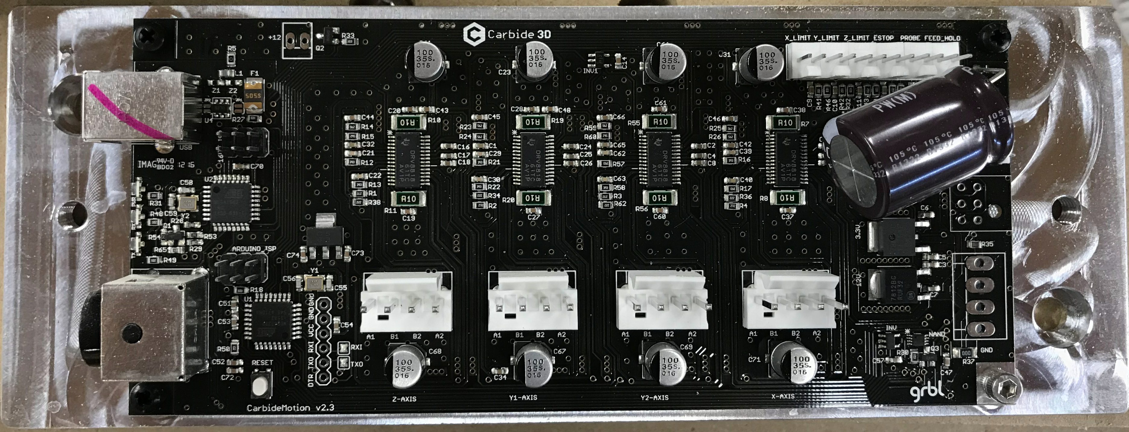
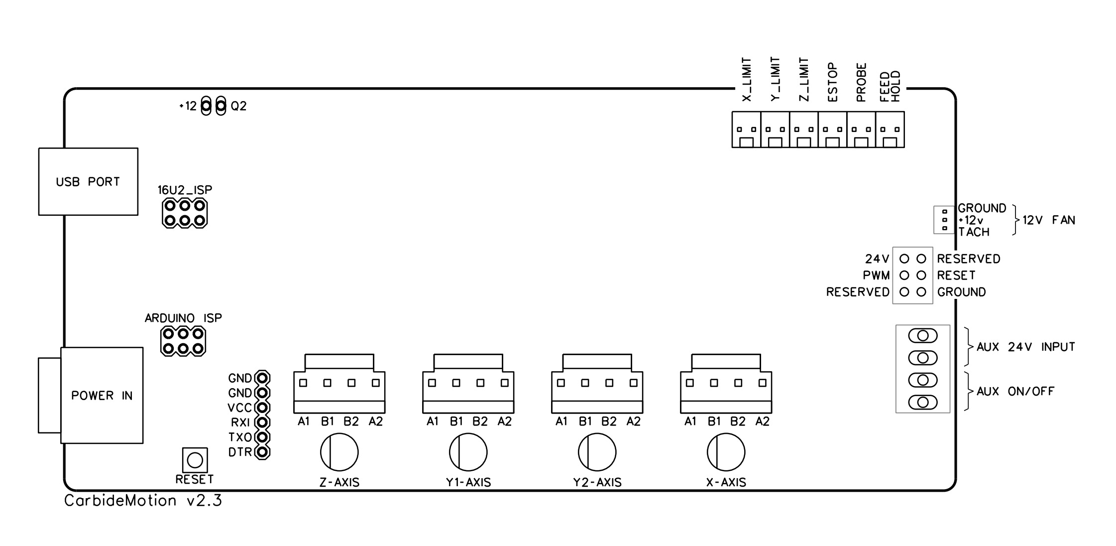
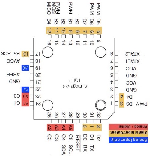
I was scouring the forum and wiki about a month ago looking for information on the v2.3 control board. I thought that maybe, maybe, it might be helpful to someone else to have all of the information I found in one location. Attached you will find a pinout diagram and a reference photo of the v2.3 board. If anyone has any extra information to be added, particularly the identification of the individual pins under “ARDUINO_ISP” and “16U2_ISP,” I would be very grateful if you posted below. I hope this is useful to someone out there.
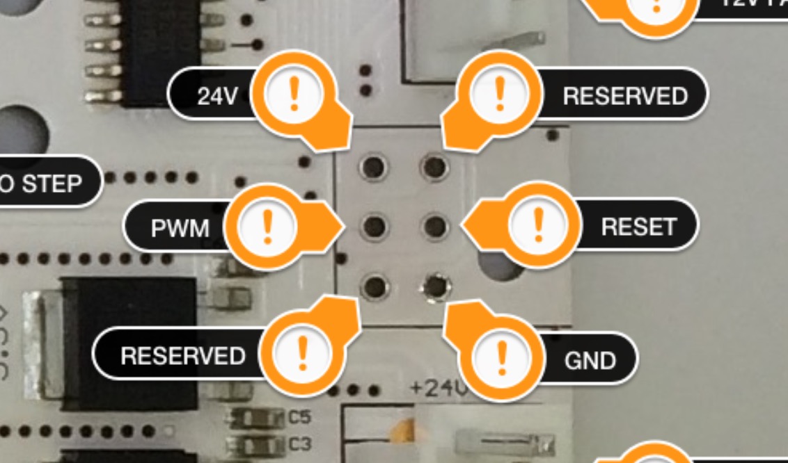
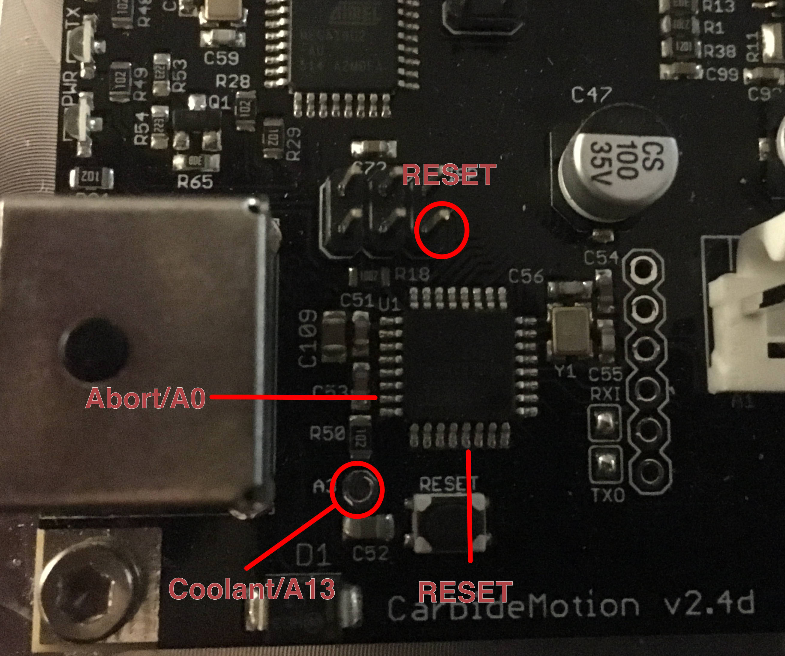
“Q2” is not a pin, is the reference designator for the transistor next to that via - I will assume for the time being that via is GND. It appears that the output of this connector is switched (hence the transistor), but I don’t know by what. A3/Coolant would make sense, but I have not verified that.
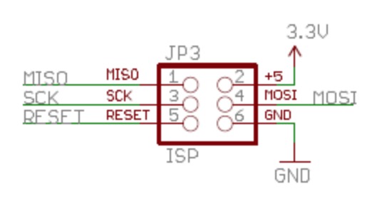
The 2 ISP sockets are just like any arduino “ISP” socket. They look like this:

This one: “16U2_ISP" is for the USB interface. You probably don’t need to touch it ever.
This one: “ARDUINO_ISP” is for the atmega part doing all the work (ie. the “arduino”) - you shouldn’t need these pins as the part can be programmed via the USB interface.
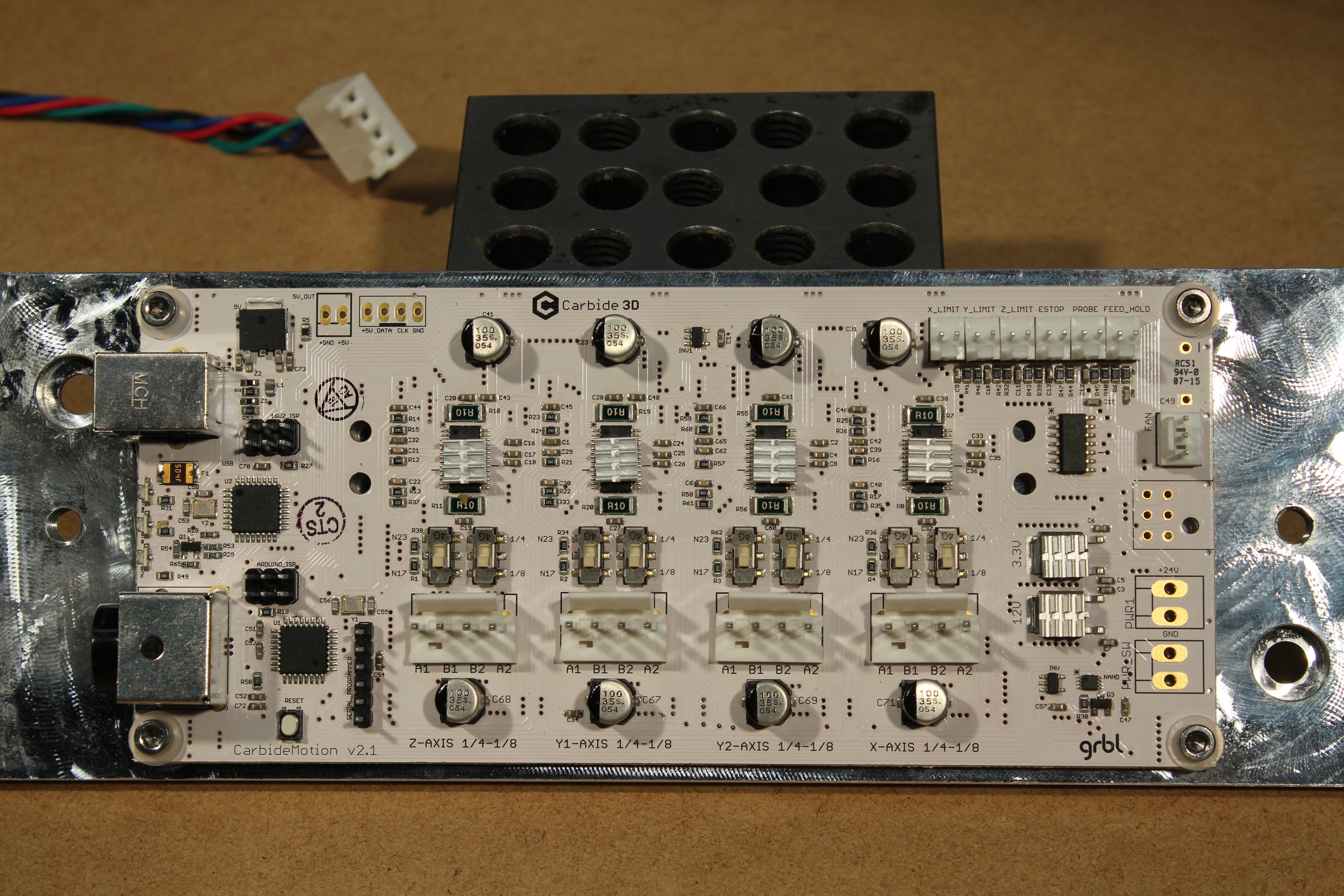
The 6 pins on the right end of the board (same on all versions)…
A3, which is coolant enable, has a via labeled “A3” over by the cpu (the atmega328 QFP toward the bottom of the board). I don’t know anyone doing gcode controlled coolant, so that’s interesting to be pulled out like that.
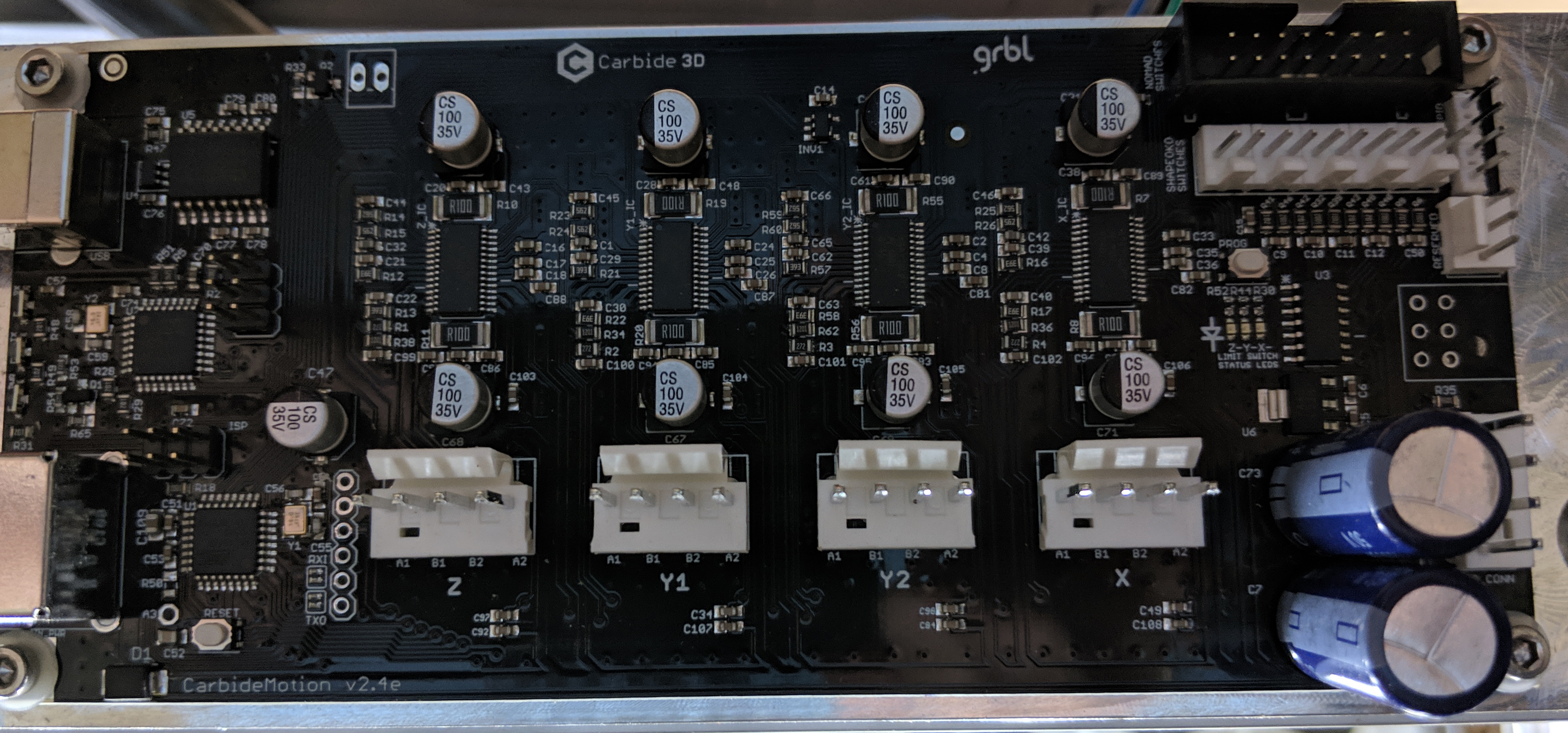
The PWM output is nicely labeled on 2.4d/e. There are 4 pins above the spindle connector, labeled PWM, 5V, GND, and D13. D13 is spindle direction on GRBL 1.1
3.The 2 pins above the “spindle connector” are for an unneeded fan. The 4 pins below it are for aux 24v input power like on the white 2.1 board.
@WillAdams I did find that resource, and the schematics on the Sparkfun website, but since my understanding of electronics is veeeery shallow it wasn’t, uh, helpful to me.
@mikep That is a lot of good info. I will incorporate the relevant information into my v2.3 schematic.